Introduction
In this mini project, we learned how to design simple circuits and PCBs using KiCad, a free software suite for electronic design automation. The circuits created here are simple, as the focus was not to design an intricate PCB but to familiarize oursleves with the program. The hope is that we will be able to use this software in the future to design custom PCBs to use in our own main project. Here's how it went-
Initial Electronics Design Practice
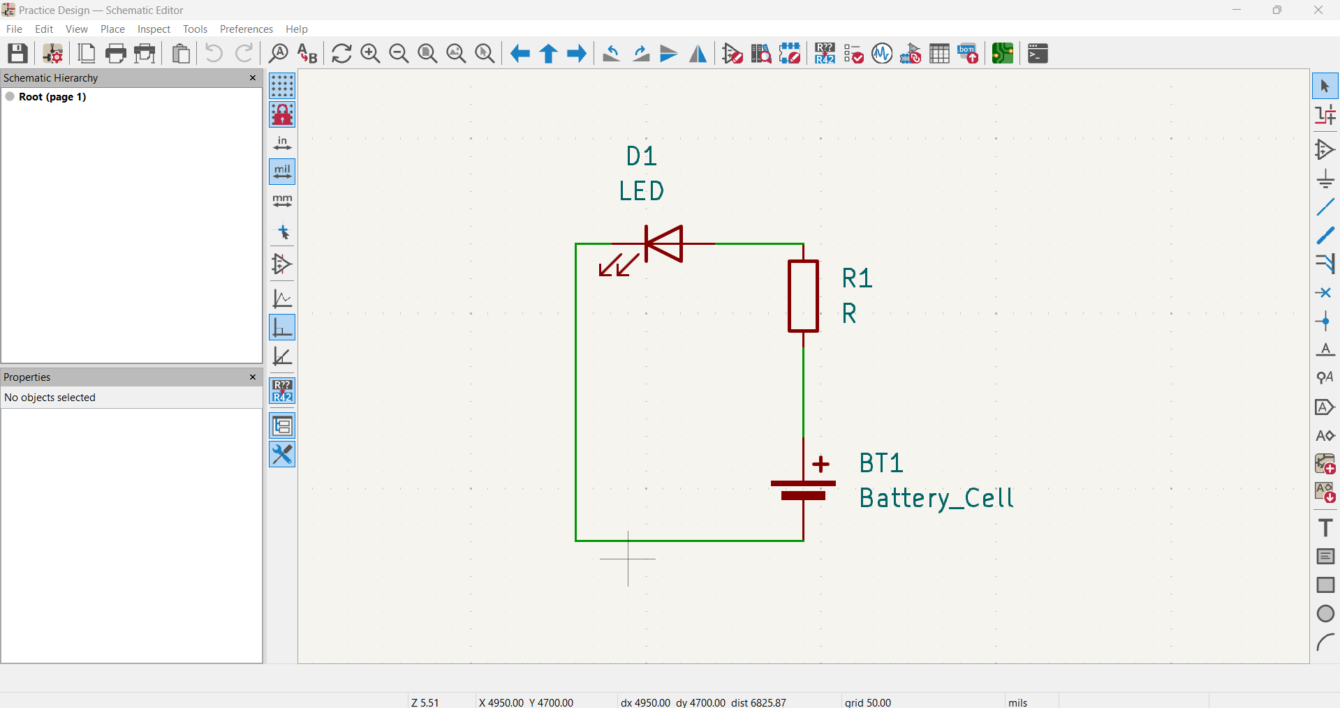
After downloading KiCad, I began the process of learning to use the program by creating a new project and opening the schematic editor. I noticed how this software functions by opening a new window for every new, editor or viewer opened, which was something that I liked, as it let me go back and forth between different parts of the program easily. I already had some experience working with circuitry, which helped me figure out the software. I looked around the schematic editor until I found the "Add Symbol" button. The instructions only involved having a battery, a resistor, and an LED in the circuit, so I added those three symbols and connected them with wires.
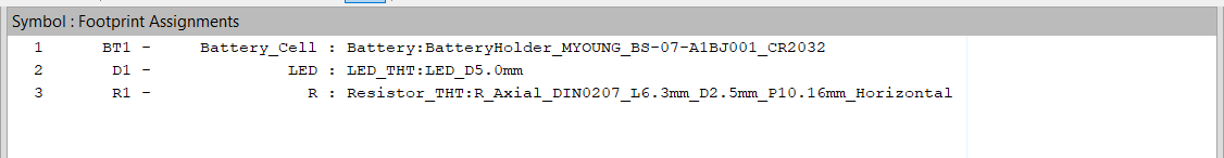
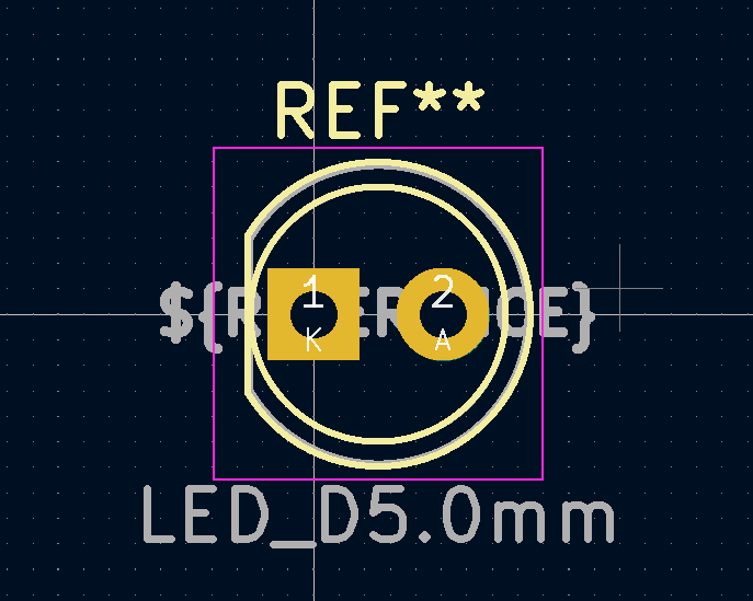
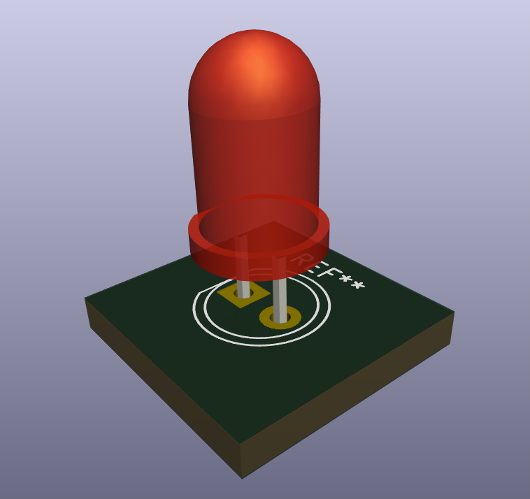
Next, I clicked on the "Assign Footprints" button at the top, which let me tag thje different components I used in my circuit with a footprint, which defines "the copper connections between physical components and the routed traces on a circuit board," (KiCad website). An exaample of this is shown below with the LED footprint.
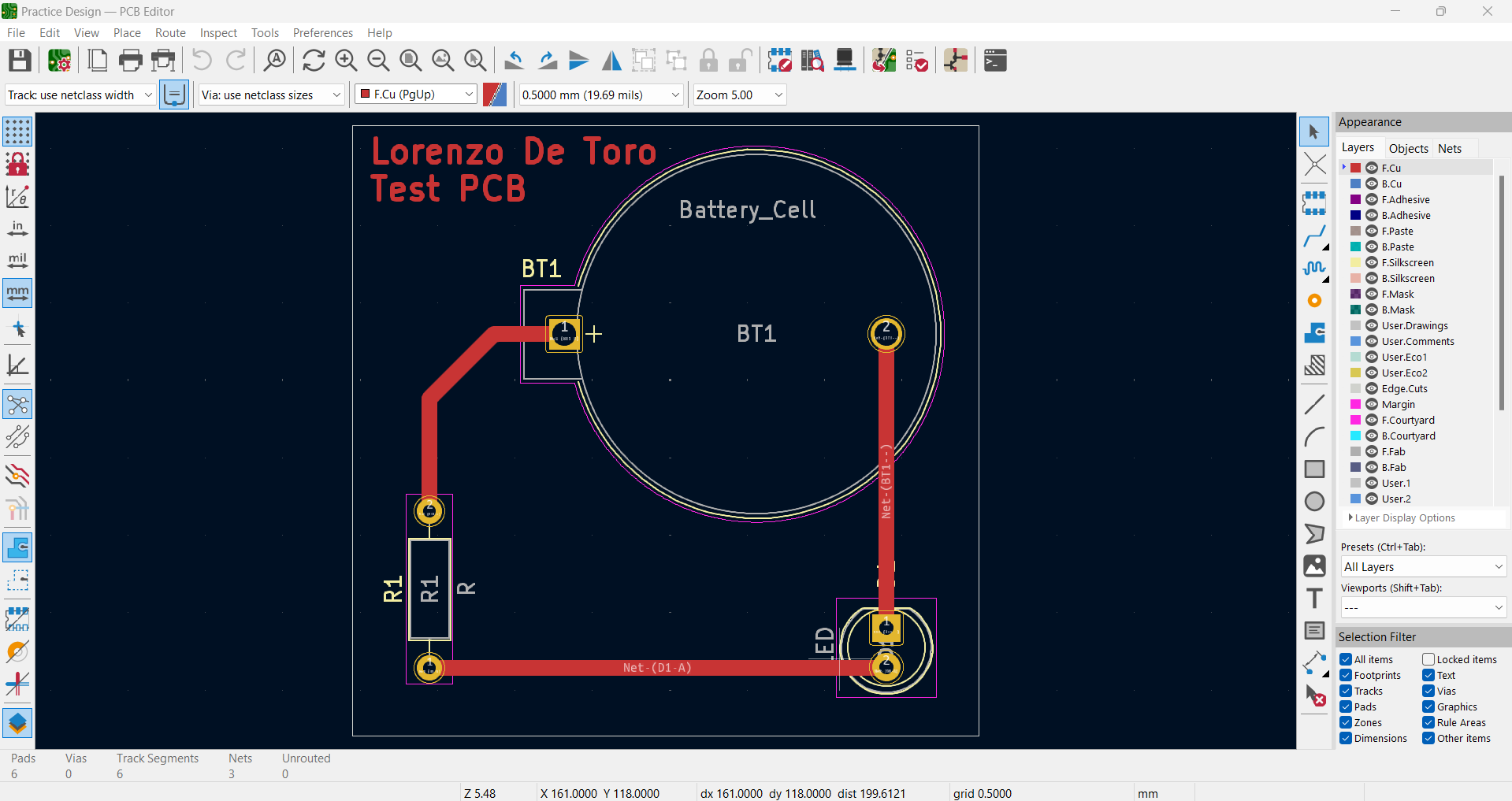
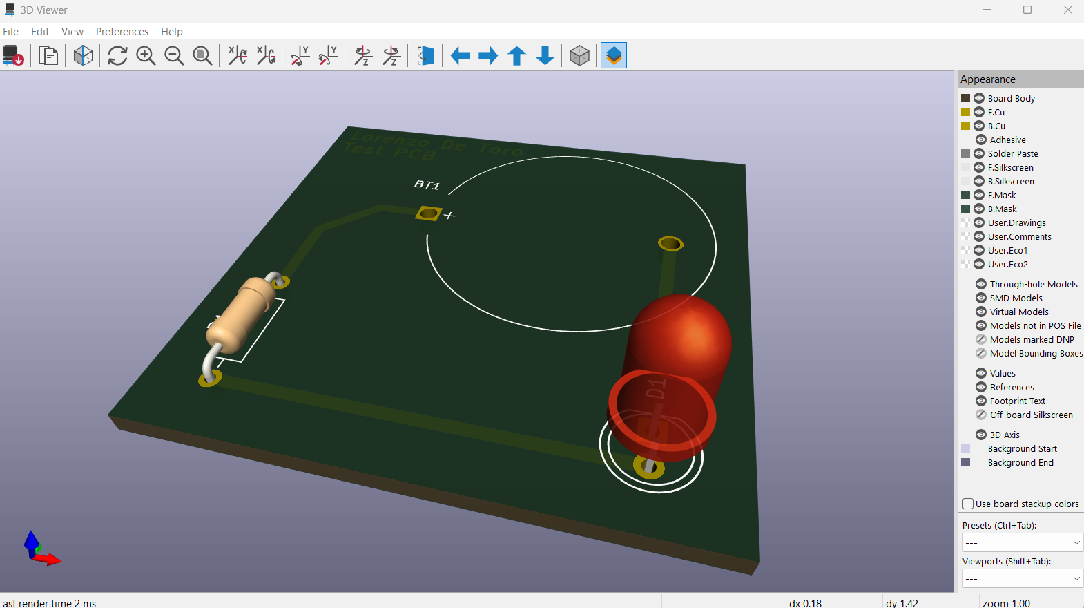
Next, I went into the PCB editor, where I finalized the PCB design for my simple circuit. First, I organize the different components that will go on the PCB, placing them in a neat way that ensures the copper line connections don't overlap. After that, I go to add the lines of copper that will act as wire for the components on the PCB. In this program, different color layers are used to tell the computer what, where, and how to cut. I use the red F.Cu layer to make the traces on the PCB. They initially came out thin, so I scaled them up to 1 mm thick. Finally, I added the outline of the PCB on the light gray Edge. Cuts layer. The next images show the final PCB shcematic and the 3D rendering of the PCB. This wrapped up my initial practice design using KiCad.
More Practice: Two Button System
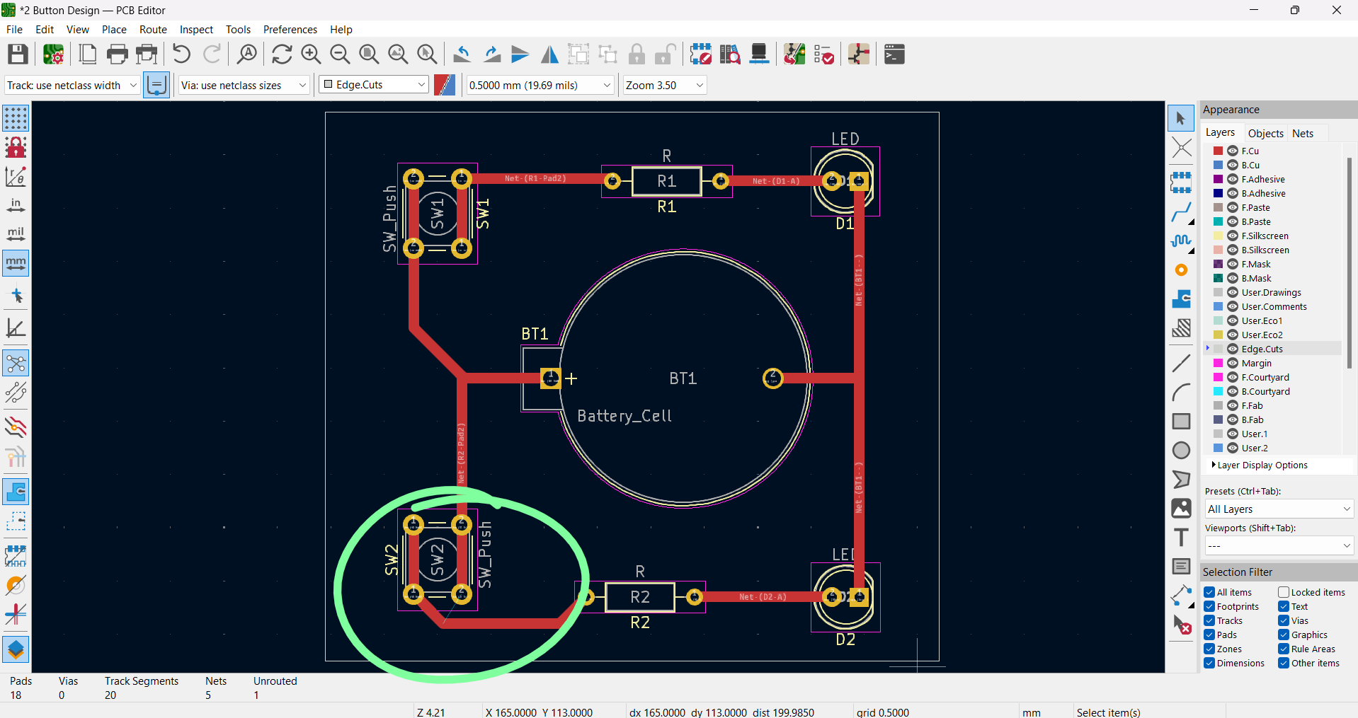
To garner more experience, we were instructed to create another circuit within our group. This time, had to include two LEDs, two resistors, a single battery, and two buttons. I took charge of this design, and decided to go with two LEDs in parallel, each being activated independently by the button in front of it. Again I began in the KiCad schematic editor, adding the appropriate symbols and organizing the schematic layout neatly before connecting everything with wire. I also assigned footprints to each component I used.
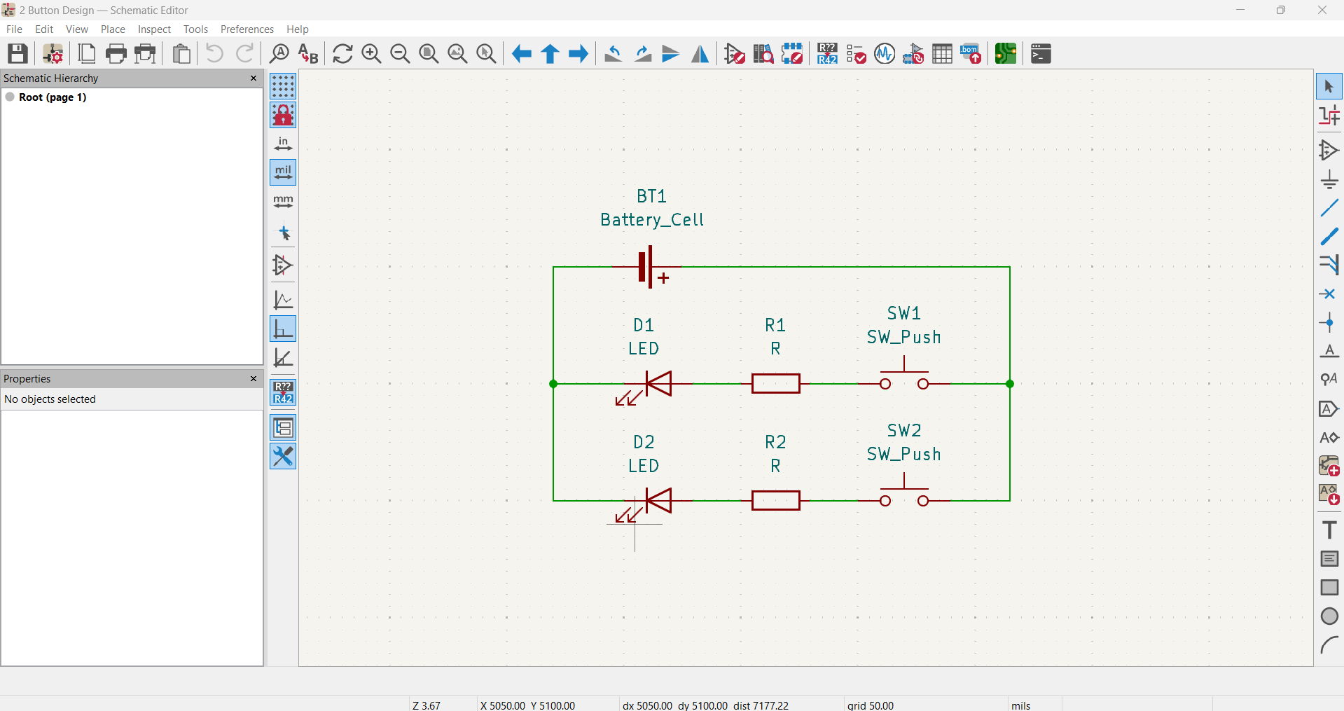
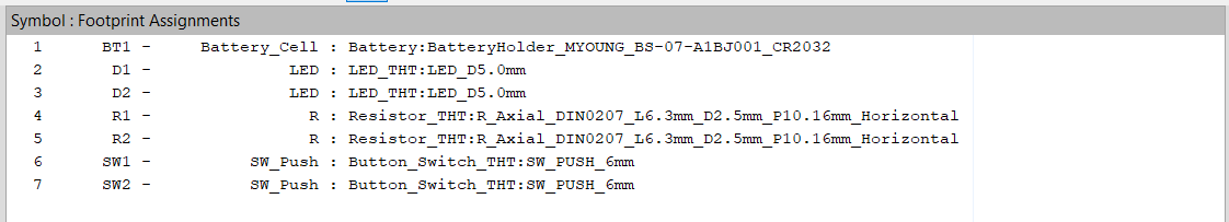
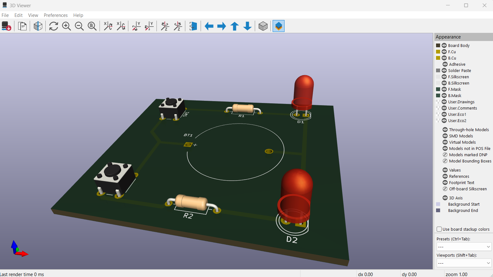
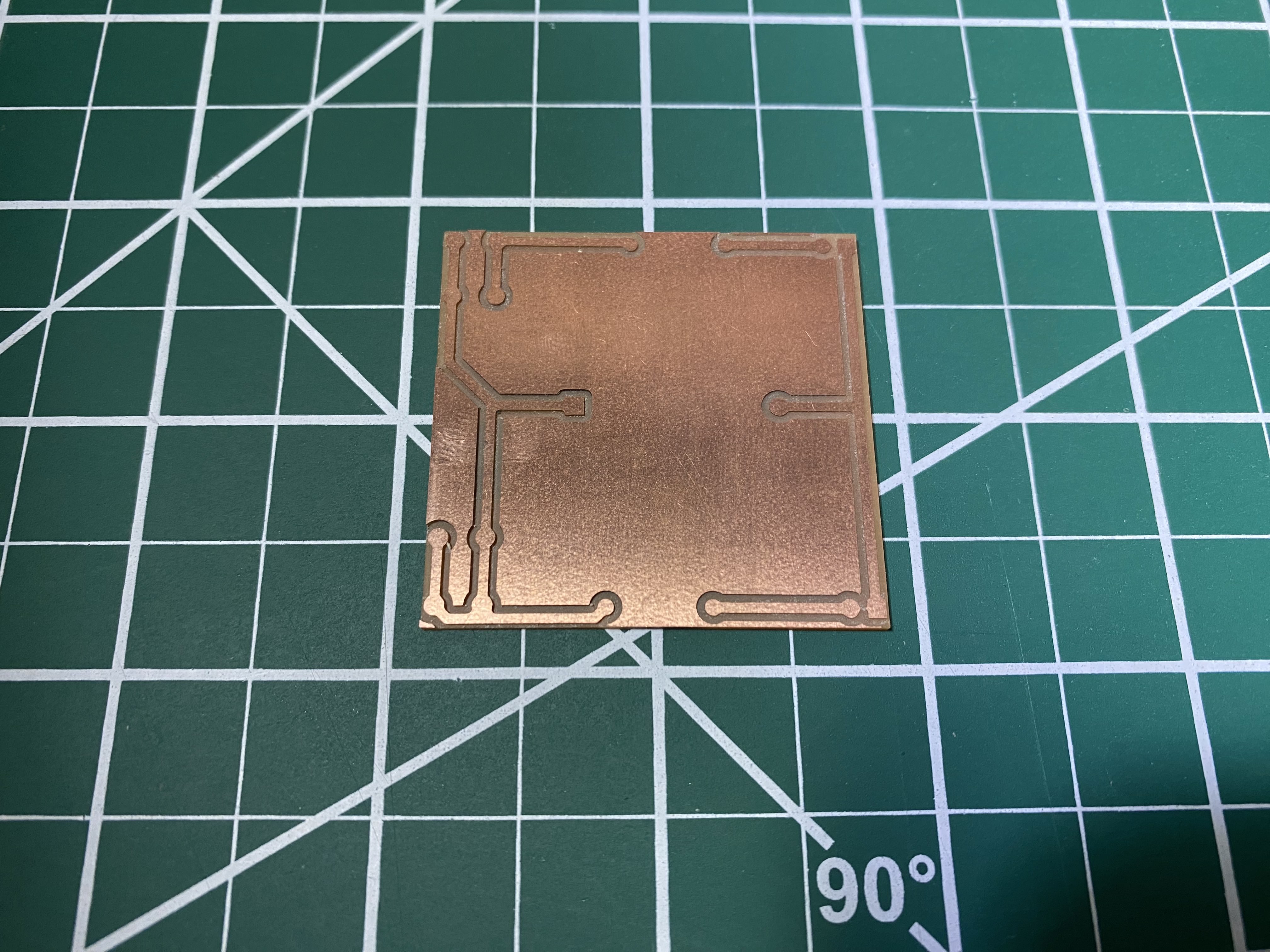
All I had to do at this point was finish the PCB editor. Like before, I organized the components, making sure none of the traces would overlap. Then I added and thickened the copper traces, and added an outline to the PCB. The next images show the final PCB schematic, a 3D render of the PCB, and the actual PCB which was cut using a CNC machine at my school. There was an issue with the files where the outline wasn't read correctly, so the PCB came out smaller than intended.
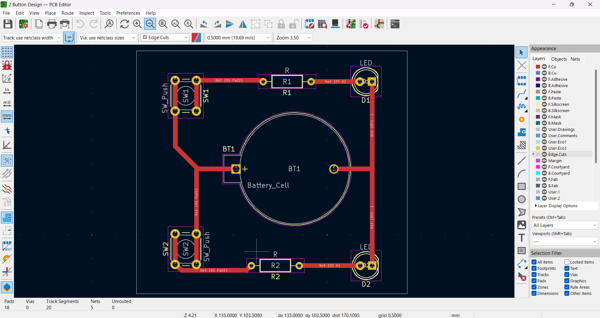
While finsihing this page, I also realized that the copper traces in the bottom left corner where the button should sit were too close together, creating a birdge that would close the circuit and remove the utility of the button. I quickly went back into KiCad and moved the wire line to fix this, giving the two traces enough of a gap between to not close the circuit, as shown in the image below.